FROM INNOVATION TO ENERGY EFFICIENCY

Our innovations in wafer production have a strong impact on increasing the energy efficiency of chips. This has a particular impact on smartphones, computers including servers, household appliances and electric vehicles.
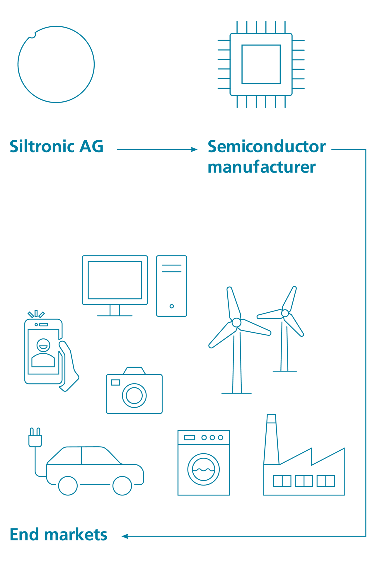

Siltronic AG

  • Hyperpure silicon wafers are the basis for almost all semiconductor devices and consequently represent an essential basis for the world’s electronics industry.


Manufacturers of semiconductors

  • Our wafers are very closely linked to computer chips because our customers – the manufacturers of semiconductors – transform wafers into chips through physical and chemical processes.


End markets

  • The most important end markets for demand for our wafers are smartphones, computers, servers, consumer electronics including household appliances, industry and automobiles. Almost all of our wafers go to these six end markets.

Annual report

Audited information and key figures on sustainability at Siltronic can be found in our current annual report.


Research and development for environmental innovations

Our research and development is aimed in the following directions in order to contribute to environmental and climate protection with our products:


Increasing the energy efficiency of chips

The power consumption drops significantly when our customers are able to integrate smaller transistors and shorter conductor tracks into wafers. The resulting increase in the chip’s energy efficiency is usually so high that a new chip operates with significantly more power than its predecessor while requiring significantly less energy. This means that more computing power can be achieved per watt. In order to achieve this, wafers must meet constantly and significantly increasing physical and chemical requirements. Meeting these increasing requirements also offers our customers the advantage of being able to produce more chips from one wafer. As chip production on the customer side is very energy and water intensive, these wafers reduce the customers' energy and water requirements. To this end, we spend many millions of euros each year on research and development and generally invest large sums in new machines. Only with state-of-the-art machines is it possible to produce technologically leading wafer types. Slightly more than half of our sales are accounted for by these types of wafers.

Innovation for electric vehicles

We are developing a new type of wafer with gallium nitride. The resulting wafer type should make the charging process for electric vehicles and other devices considerably more energy-efficient and faster. It would also increase the range of electric vehicles.

Wafers for controlling current flows

Certain types of wafers are used to produce chips that control current flows. These are also known as power chips or power semiconductors. Without power chips, for example, modern household appliances would be unthinkable, LED lighting as we know it would not exist, nor would small power supply units or chargers. Almost one third of our sales relate to wafers used for power semiconductors.

Energy efficiency of electronic products

To make power semiconductors more energy-efficient, we have developed special wafer materials with a low oxygen content. Chips of this type have a power-saving effect in devices in which high direct and alternating currents are converted. Examples include the current flow between the electric motor and the battery in a fully electric car, between a charging station and an electric vehicle or between the power grid and the generation of electricity from renewable energies (primarily wind turbines, photovoltaics). Without the provision of special wafer materials, the energy efficiency of many electrical products, including electric vehicles, would be significantly lower. Wafer types made from these special wafer materials account for slightly more than 15 percent of our Group sales.


Cooperation with customers as the key to success

Many of our projects require close and continuous cooperation with our customers. To this end, we work on projects with our technologically leading customers as part of joint development programs, taking care to cover a broad spectrum of semiconductor end applications. We also work together with research and academic institutions.